
Archived — final / last release. This project is complete and frozen. Issues and PRs are not expected; the tree is the historical record.
A hand-designed Altera MAX 7000AE/S CPLD development board and the digital labs built on it — from Lake Washington Institute of Technology Electronics 211 (2017–2018), by James Burney (K9DTV).
This repository packs the PCB design, fabrication outputs, board photos, project write-ups, and Quartus calculator / board-test projects that targeted the board.
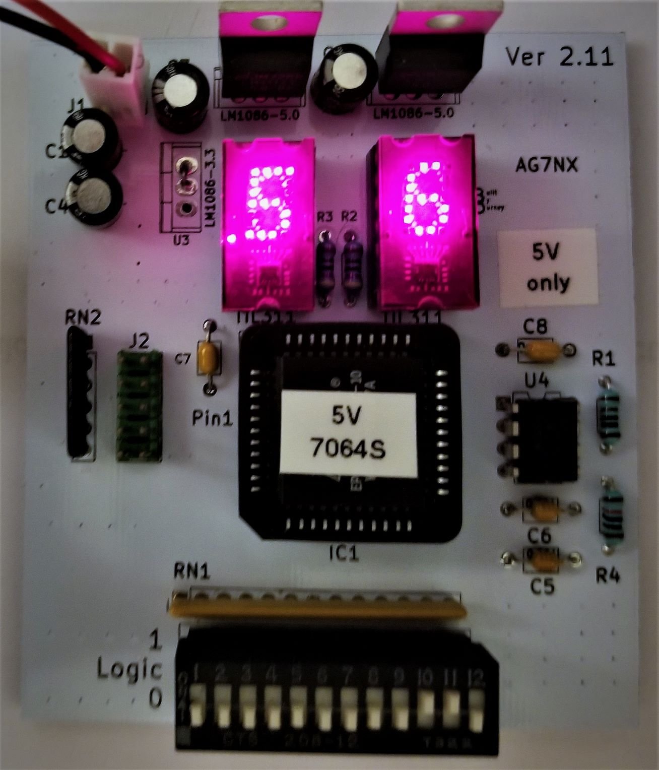
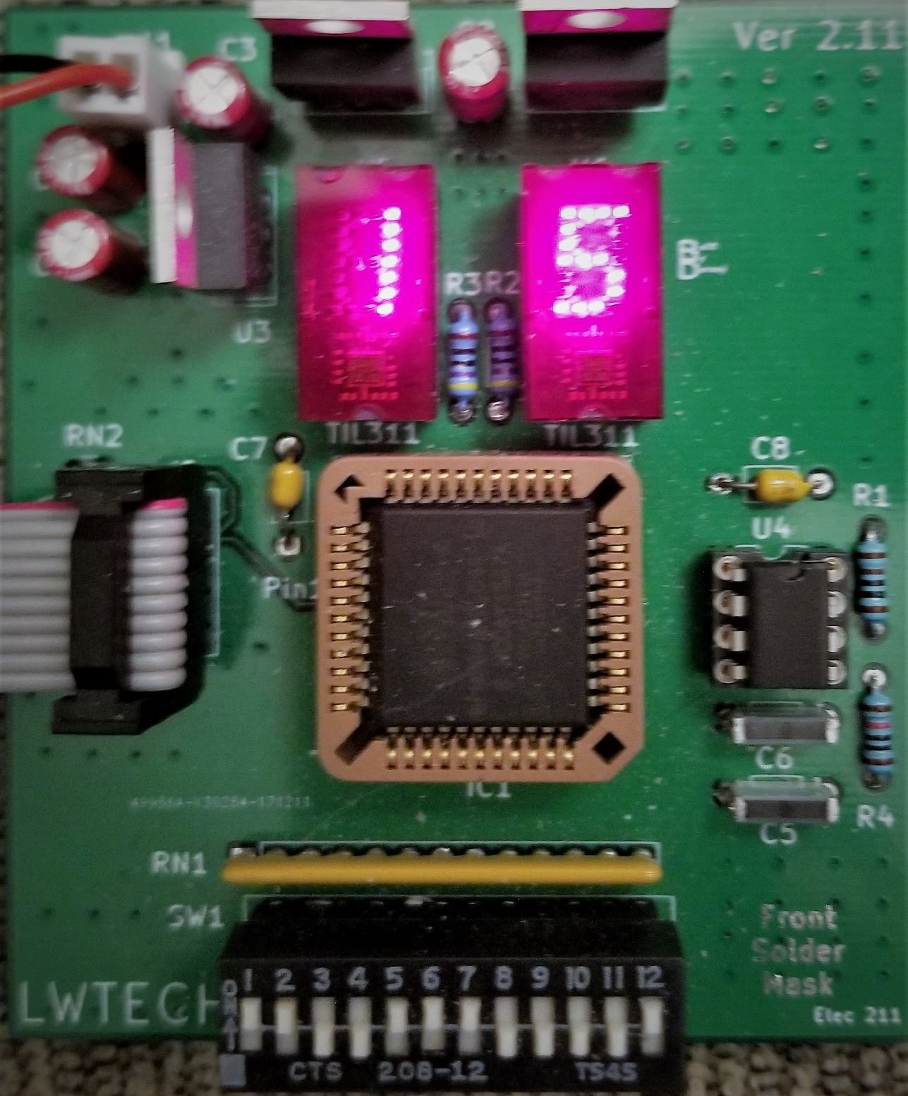
Left (white / Ver2): board pictured with the MAX 7000S 5 V CPLD setup. Right (green): Ver1-style build.
What this board is
The goal was a durable printed CPLD trainer for the same class work that started on a hand-wired prototype: DIP switches in, dual hexadecimal TIL311-style displays out, on-board clock, and a standard JTAG/ByteBlaster programming header.
Two PCB revisions shipped:
| Version | How to spot it | Notes |
|---|---|---|
| Ver1 | No silkscreen | Used for most lab examples in the docs |
| Ver2 | Has silkscreen | Three display-control pins remapped (see pin table below) |
Power: about 6.5 V–12 V input (prefer the low end; regulators get hot). Current-limit around 160 mA when using a bench supply. Drive each display decimal point with an open-drain buffer so the DP turns fully off.
MAX 7000S (5 V) vs MAX 7000AE (3.3 V)
Same PLCC-44 socket and the same lab/pin idea. The difference is supply voltage / family:
| Family | Example parts | Core / I/O | Notes |
|---|---|---|---|
| MAX 7000S | EPM7032, EPM7064S | 5 V | White board photo; use Calculator-full-5v |
| MAX 7000AE | EPM7032AE, EPM7064AE | 3.3 V | Use Calculator-full-3v3 |
Same calculator logic in both folders — pick the build that matches the CPLD voltage. Do not mix a 5 V part with a 3.3 V rail (or the reverse) without checking VCCIO/VCCINT wiring.
Supported CPLDs (PLCC-44):
- EPM7032 / EPM7032AE (32 macrocells) — display/switch / board-test labs
- EPM7064S (64 MC, 5 V) —
calulator/Calculator-full-5v/ - EPM7064AE (64 MC, 3.3 V) —
calulator/Calculator-full-3v3/
Repository layout
.
|-- README.md
|-- cpld-white.jpg / cpld-green.jpg   # Assembled boards
|-- cpld-pcb.png / cpld-sch.png       # Layout / schematic views
|-- PCB-files/
|   |-- cpld/                         # KiCad schematic + PCB (legacy KiCad 4 era)
|   `-- CLPD-grb/                     # Gerbers + drill for fab
|-- calulator/                        # Quartus II projects (folder spelling preserved)
|   |-- Calculator-full-5v/           # Full calculator — EPM7064S / 5 V
|   |-- Calculator-full-3v3/          # Full calculator — EPM7064AE / 3.3 V
|   |-- board test/                   # Board bring-up
|   |-- board-test-2/                 # Switch / display exercise (32 MC)
|   `-- boardtest3/                   # Follow-on board test (uses board-test-2 BDFs)
|-- project docs/                     # Word write-ups (board build, PCB, counter, finals)
`-- homework/                         # Class notes (ELEC 211 Ch. 4)
Folder and filename spellings (calulator, CLPD-grb, spaces in project docs) match the original archive on purpose.
Hardware pin map
DIP switches are active-low (closed = logic 0). Most designs invert them in the CPLD so “switch ON” reads as a 1 in the logic.
| Function | Ver1 CPLD pin | Ver2 CPLD pin |
|---|---|---|
| DIP SW 1–12 | 4, 5, 6, 8, 9, 12, 11, 14, 16, 17, 19, 18 | same |
| Clock (~66.6 kHz from 555) | 24 | 24 |
| Display A / B / C / D | 27 / 25 / 26 / 28 | same |
| Display Blank | 29 | 29 |
| Right Latch | 31 | 33 |
| Left Latch | 33 | 36 |
| Right DP | 34 | 34 |
| Left DP | 36 | 31 |
Programming-header pins follow the usual Altera JTAG layout (not duplicated in the table).
Major bill of materials (either revision)
| Ref | Part | Notes |
|---|---|---|
| IC1 | EPM7032 / EPM7064S (5 V) or EPM7064AE (3.3 V), PLCC-44 | 64 MC for full calculator |
| U1–U2 | LM1117-5.0 | 5 V rails |
| U3 | LM1117-3.3 | CPLD I/O / core as wired |
| U4 | LM555 | ~66.6 kHz board clock |
| U5–U6 | TIL311 (or DIS1417) | Hex displays (hard to source; eBay) |
| SW1 | 12-position DIP slide | Active-low inputs |
| RN1 / RN2 | 10 kΩ SIP arrays | Pull-ups |
| J2 | 2×5 header | Programming |
Full Digi-Key / Mouser part numbers are in project docs/pcb document and cpld project.docx.
Labs and example designs
Documented in project docs/:
- Board bring-up — display blank/latch behavior, 555 clock divider blinking both DPs (~1 Hz after ÷65536). Quartus:
calulator/board test/. - Priority encoder — exercises all DIP switches into the hex displays (BCD).
- Calculator (needs 64 MC device) — mode select on SW11/SW12:
- SW11=0, SW12=0 → min/max (7485-style compare; DPs show a swap)
- SW11=0, SW12=1 → add
- SW11=1, SW12=1 → subtract (borrow aware)
- SW11=1, SW12=0 → multiply
Calculator-full-5v/(EPM7064S, 5 V) andCalculator-full-3v3/(EPM7064AE, 3.3 V). - Two-digit counter — final-style exercise on the same pinout (
two digit counter cpld project.docx). - Hand-wired prototype — earlier 7000-series socket board used for Ch. 4 / Ch. 7 (
211 build board.docx).
Quartus project (calulator/)
Intel/Altera Quartus II block-diagram labs. Folder name spelling calulator is preserved. The calculator top entity is named Calculator.
Full calculator (two voltage builds)
| Folder | Device | I/O | Fit | Use when |
|---|---|---|---|---|
Calculator-full-5v/ | EPM7064SLC44-10 (MAX7000S) | TTL (5 V) | 60 / 64 MC | 5 V CPLD (white board photo) |
Calculator-full-3v3/ | EPM7064AELC44-10 (MAX7000AE) | 3.3-V LVTTL | 60 / 64 MC | 3.3 V AE CPLD |
Each folder has its own Calculator.qpf, BDFs/BSFs, Calculator.pof, and reports. Ver2 display pins. Open the folder that matches the chip on the board.
Board tests
| Folder | Role |
|---|---|
board test/ | Bring-up (boardtest.qpf, .pof included) |
board-test-2/ | Switch/display lab (board-test-2.qpf, EPM7032AE, .pof included) |
boardtest3/ | Later board test (test3.qpf; BDFs from ../board-test-2/) |
Suggested tools: Quartus II 13.0 SP1 (or 17.1 Lite) with a USB-Blaster.
KiCad / fabrication (PCB-files/)
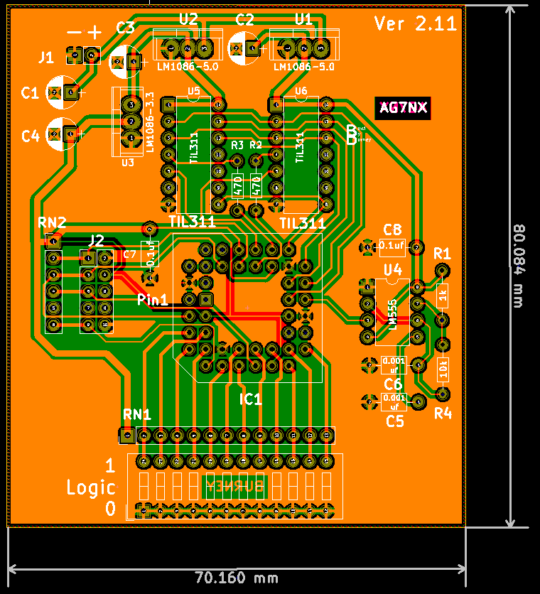
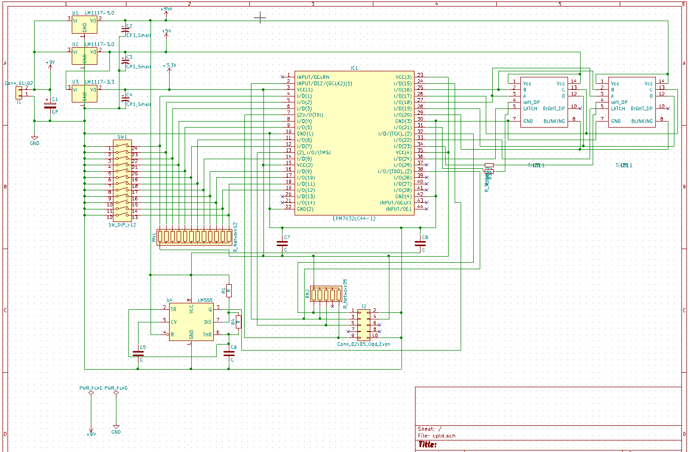
PCB-files/cpld/— schematic (.sch), board (.kicad_pcb), netlist, project (KiCad 4-style.pro).PCB-files/CLPD-grb/— Gerber layers (F/B Cu, mask, silk, edge cuts) andcpld.drl.
Open with a modern KiCad via the legacy importer, or send the Gerbers straight to a fab.
Documentation (project docs/)
| File | Contents |
|---|---|
211 build board.docx | Hand-wired prototype + Ch. 7 calculator path |
pcb document and cpld project.docx | Ver1/Ver2 PCB, pin map, BOM, calculator labs |
two digit counter cpld project.docx | Counter lab on the PCB |
211 PROJECT.docx / 211 final.docx | Course project / final write-ups |
Course context: Lake Washington Institute of Technology, Electronics 211, instructor Professor Peter Welty.
License / provenance
MIT on GitHub. Personal educational hardware and reports by James Burney (K9DTV). Course homework notes in homework/ are included as archived class material. Altera/Intel tool output remains under their respective license terms.
Site / contact: k9dtv.com · GitHub: K9DTV/cpld-development-system
Archived from the original CPLD development-system materials (2017–2018) and published as a public K9DTV project.